Photoelectric Characteristics Of Nano TiO2 Film Prepared By Spraying Pyrolysis Method
Cuong Tran Kim
Department of Natural Sciences, Ho Chi Minh City University of food Industry, Vietnam.
*Corresponding Author
Cuong Tran Kim,
Department of Natural Sciences,
Ho Chi Minh City University of food Industry,
140 Le Trong Tan Street, Tan Phu District, Vietnam.
E-mail: cuongtk@cntp.edu.vn
Article Type: Review Article
Received: April 07, 2015; Accepted: May 06, 2015; Published: May 08, 2015
Citation: Cuong Tran Kim (2015) Photoelectric Characteristics of Nano TiO2 Film Prepared by Spraying Pyrolysis Method. Int J Nano Stud Technol.4(1), 78-83. doi: dx.doi.org/10.19070/2167-8685-1500015
Copyright: Cuong Tran Kim© 2015 This is an open-access article distributed under the terms of the Creative Commons Attribution License, which permits unrestricted use, distribution and reproduction in any medium, provided the original author and source are credited.
Abstract
The nanocrystalline TiO2 (nc TiO2) film was prepared by spraying pyrolysis method. Starting material for the synthesis was TiCl4. Phase compositions and crystalline sizes were examined by pattern of XRD, and surface morphology of the thin film was analyzed by SEM and AFM. Optical characteristics were examined by UV – Vis and luminescent spectra (PL). Electric characteristics were examined by measuring resistance changing of films versus temperature. The experimental data showed that the forming films had nanostructure and typical photoelectric characteristics of nano TiO2 material which is similar to the ones prepared by other preparing methods. IF compared to others, this preparing method has such as simple equipments, inexpensive and available materials; so it is suitable for mass production.
2.Experiments
2.1 Materials
2.2 Apparatus
2.3 Apparatus for preparing nano TiO2 by spraying pyrolysis method
3.Results and Discussion
3.1 Structure and morphology of nano TiO2 films
3.2 Optical characteristics of nano TiO2 films
3.3 Electric characteristics of nano TiO2 films
4.Conclusion
5.References
Key Words
Nano TiO2 film; Spraying Pyrolysis Method.
Introduction
Nano titanium oxide has a lot of applications in real life. It is used to make dye in industry to produce paint, plastic, paper and food products. TiO2 has been even covered on interior furniture to create reflected light effects which increase their beauty, etc. Together with development of nano material technology, at present, there are important applications of nano (nc) TiO2 including photocatalysis, solar cells, photon and photoelectron devices, etc. With oxidation potential is 3.2 eV, under effect of ultraviolet light (UV), nc TiO2 can decompose very strong toxic wastes in environment.
TiO2 was used as an insulating gate on the field effect transistor (FET) [15], to make detectors for measuring nuclear radiations [2], and to make luminescence devices [4]. When doping more appropriate impurities, it will create energy levels of Ea located in the bandgap. If electrons simultaneously jump from excited levels to elementary energy levels, the material shall generate desired radiations. The change of color windows act based on this principle. The impurities energy levels can be controlled by electric field; therefore, we have color changing instantaneously depending on the control of the electric field [10, 20]. TiO2 was also used to make anti reflexing layers help enhancement of efficiency of photosemiconductor amplifiers (laser) GaInAs/AlGaInAs [12]. Because TiO2 has very large refractive index, fiber optic cables or optic windows covered this material, which acts based on continuous reflection principle, will produce total reflect, which will minimize the loss of light (sign).
There have been different methods used to prepare nano materials and nano films from relatively simple to rather complex including physics methods (Physical vapor deposition – PVD), chemical methods (Chemical vapor deposition – CVD) and many others such as physics and chemical combined method or combined different methods.
Spraying pyrolysis method (SP) is one of the most simple and economic methods to prepare oxide metals. Using nano TiO2 films prepared by SP method and using inexpensive materials can enhance applied ability of this material [1]. Besides the simplicity of the method, low cost with a minimum amount of waste, SP process even permits to prepare cover layers with large areas and easily apply for industrial manufacture [8]. This is remarkable advantage of SP method compared to other methods.
SP method has been used by many authors to prepare nano TiO2 films including single atom films and polyatomic films from different starting salts. Actually, the authors [18] sprayed pyrolysis liquid mixture of titanium and niobium peroxo-hydroxo on quartz substrate to prepare oxygen sensitive sensor. Another authors [5] prepared TiO2 films and carbon doped TiO2 powder using starting material was titanium-tetraisopropoxide, the obtained films have anatase single phase structure, the average size of crystalline particles was ~ 160 nm. Additionally, the authors [1] prepared TiO2 films on glass substrate using titanium (IV) isobutoxide [Ti ((CH3)2CHCH2O)4] as starting material. Also, the authors [19] prepared TiO2 films on glass substrate using starting material of C10H14O5Ti, the obtained films have the crystalline particle size from 30nm to 50nm. The authors starting material of C1[17] prepared TiO2 films by starting materials of TiCl3 solution. The authors [4] prepared TiO2 films by using titanium diisopropoxide as starting material, the average size of crystalline particles was ~ 210nm.
Experiments
TiCl4 was prepared into solution with concentrations ranging from 0.025 to 0.15mol/dm3 (M). The solution was sprayed with atmosphere-pressing pressure 1.5 at. Substrates were made by optical glass with thickness of 1.2mm. Substrate temperatures were studied ranged from 340°C to 460°C.
X-ray diffraction patterns (XRD) of nanocrystalline TiO2 films were measured by a D8-AVANCE BRUKER X-ray diffractometer using Cu Kα radiation (k = 0.1542nm) with 0.02°/sec scan rate. Field effect scanning electron micrographs (FESEM) were taken with a FESEM HITACHI S4800 field effect scanning electron microscope. Atom force micrographs were taken with a Multimode-VEECO-USA atom force microscope. UV-Vis absorption spectra were measured by a Shimadzu UV-Vis 2540 absorption spectrometer. Luminesce spectra were measured by a FL 3-22 Jobin – Yvon – Spec., USA.
This apparatus are self-prepared. Scheme of nano TiO2 film preparing system by spraying pyrolysis deposition method was showed in Figure 1. Temperature controlling system used digital technology of OMRON company with degree of displaying accuracy of 1°C. Steam pressure was controlled by two compressed valves of UniD800 (Taiwan). Spraying frequency was controlled by electronic IC system which may control all of pulse to alter not only spraying time but also pausing time.
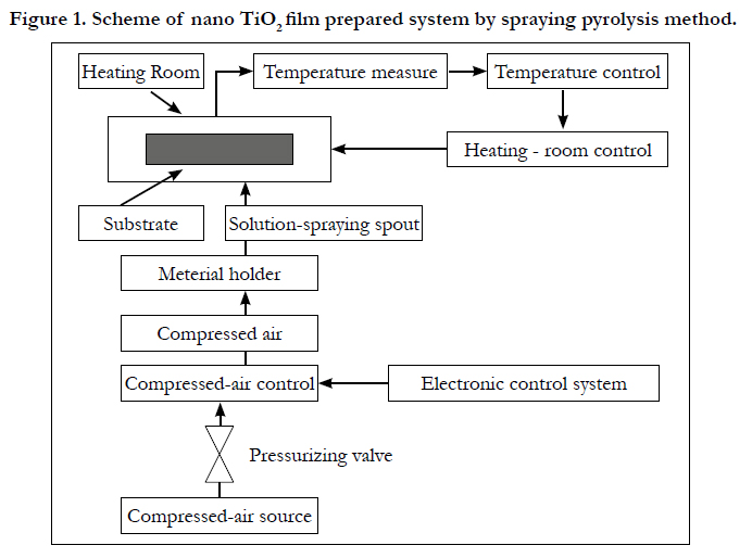
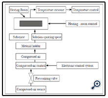
Figure 1. Scheme of nano TiO2 film prepared system by spraying pyrolysis method.
Results and Discussion
The crystalline phase of ellipsoidal TiO2 was characterized by Xray diffractometer. Figure 2 shows the film XRD pattern deposited from spraying pyrolysis deposition method at 380°C with solution concentrate of TiCl4 = 0.03M. The XRD pattern shows that Bragg reflections were very clear at typical diffraction angles 2θ = 25.4°, 38.8°, 48.0° and 55.0° corresponding to crystalline planes: (101), (112), (200) and (211), they were the same as results of the authors [11]. All of the films had single phase anatase structure.
Figure 2. The XRD pattern of TiO2 film prepared from spraying pyrolysis deposition method at 380°C.
Figure 3 shows the XRD patterns of the films prepared at different substrate temperatures at the same experimental condition. The XRD patterns showed that at the studying temperature range of 340 – 460°C, all of the formed films had single phase anatase structure.
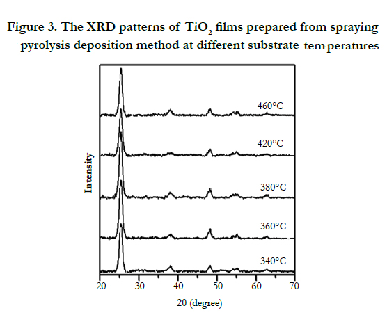
Figure 3. The XRD patterns of TiO2 films prepared from spraying pyrolysis deposition method at different substrate temperatures
The surface morphologies of the film deposited at 450°C are shown in Figure. 3 and 4. From the profiles, it can be observed that the film is porous nanostructure with the average grain size of about 20nm. This relates to evaporation process of solvent and semi-finished product in the pyrolysis process from starting material. Image of Scanning electron micrograph (SEM) of the typical pattern prepared by solution concentrate 0.1 M and at temperature of 450°C is shown in Figure. 4 and its atomic force micrograph (AFM) are shown in Figure 5.
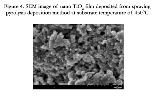
Figure 4. SEM image of nano TiO2 film deposited from spraying pyrolysis deposition method at substrate temperature of 450°C
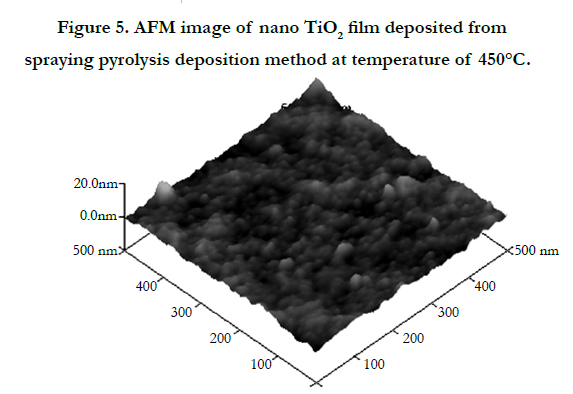
Figure 5. AFM image of nano TiO2 film deposited from spraying pyrolysis deposition method at temperature of 450°C.
The SEM shows the particles are distributed relatively homogeneously and mesoporously. This result agrees with the SEM of nano TiO2 film of authors prepared by different methods [6, 7].
The AFM image shows that size of crystalline particles obtained in this work relatively uniform at the range ~ 10 – 15 nm, rough-ness of film was about 100nm, there were a lot of holes inside the film. Combined with SEM image, it can be seen that sizes of holes varied on a large scale – in range from ~ 20 nm to ~ 200 nm. The formed films had a very porous structure, so they may have high efficiency on applications of photocatalysis and photoelectrochemical dye sensitized solar cells.
Figure 6 shows the absorption spectrum of nano crystalline TiO2 films prepared at substrate temperature of 450°C and solution concentration of 0.1M. Absorption of the films was a function of light wavelength, it slowly increased according to decreasing of wavelength in visible light range, but in ultra violet range absorption coefficient increased very fast corresponding with level transitions band – band of electrons from valence band to conduction band of nano TiO2. The shape of absorption spectrum obtained here was the same as that of the authors prepared from TiCl3 by the same SP method [17], or from TiCl4 and Ti(SO4)2 by other methods [3, 23, 24], or from commercial nano TiO2 powder by doctor blade method [22], or of nano TiO2 particles prepared by hydrolysis method TiCl4 [14].
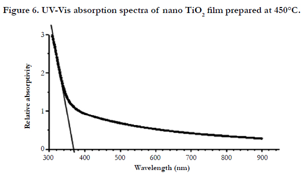
Figure 6. UV-Vis absorption spectra of nano TiO2 film prepared at 450°C.
Adsorption edge was determined by linear extrapolation of absorption coefficient α in absorption range to value 0 as well as the authors made [16]. Obtained result was adsorption edge at 370 nm, corresponding with photon energy at 3.35 eV.
From absorption spectrum, we can calculate bandgap size from expression for fundamental adsorption coefficient:
α(hγ) = A[hγ – (Eg ± hγf)]2 ------ (1)
Where hγ denotes energy of photon, Eg is bandgap energy of semiconductor, hγf denotes energy of phonon, A is constant.
The authors [6,9,17,19,23] calculated bandgap size for nano TiO2 according to Tauc model in the range of high absorption coefficient [9] by expression:
α =(A(hγ - Eg)n/2)/hγ-----------(2)
A is constant which is not dependent on energy of photon, but according to the authors [6] then A is absorption coefficient which is dependent on energy of photon for the case of nano TiO2; n = 1 for allowed direct level transitions, n = 4 for allowed indirect level transitions, n = 3 for forbidden indirect optical level transitions.
Graph expresses (αhγ)1/2 that is calculated according to absorption spectrum of nano TiO2 film in Figure 7 on photon energy of incident light was showed on figure 6. Bandgap size ~ 3.35 eV was obtained by extrapolating linearly at the absorption range with high photon energy to value α = 0. This result was in the value range of other authors [3, 23, 24].
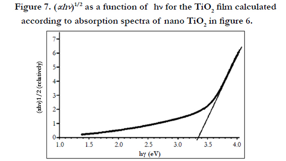
Figure 7. (αhν )1/2 as a function of hν for the TiO2 film calculated according to absorption spectra of nano TiO2 in figure 6.
Obtained Eg value was larger than that of anatase TiO2 bulk (3.2 eV). The cause may not be by nonstoichiomatric composition of nano TiO2 film, since the nonstoichiomatric composition leads to decrease in bandgap size. According to [21], a nonstoichiometry only leads to creating oxygen vacancies (Ti3+) acting as trap levels in TiO2 layers but does not lead to increasing in bandgap size. This occurs similarly to doped semiconductor. All of the authors reckoned that the increase of bandgap size for nano TiO2 prepared by different methods with different starting materials was due to quantization of size [14, 16, 22, 23]. The obtained value was in the value range of other authors for nano TiO2 films prepared by SP method from different starting materials: Eg = 3.31 – 3.36 eV from Titanyl acetylacetonate (TiAcAc) [19]. Direct bandgap size Eg = 3.1 eV from TiCl3 [17]. Eg = 2.99; 3.30 và 3.32 eV from solution of ethanol titanium diisopropoxide, corresponding to substrate temperatures were 250, 400 and 500°C [3]. Eg ~ 3.8 eV from titanium (IV) isobutoxide [1]. Indirect optical bandgap size Eg = 3.39 – 3.42 eV and direct optical bandgap size Eg = 3.67 – 3.72 eV [9].
Figure 8 shows luminescent spectrum of nano TiO2 film was excited at wavelength of 330nm. Luminescent spectrum had maximum peak at wavelength of 394.5nm.
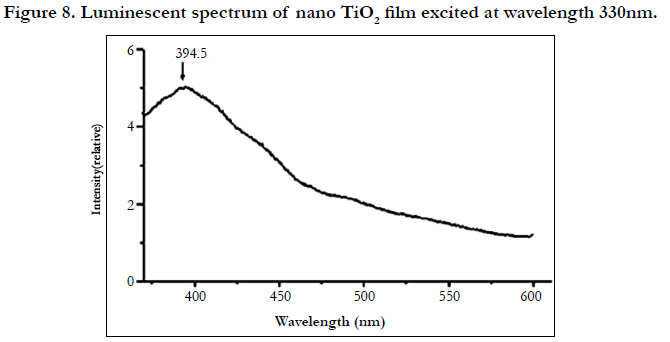
Figure 8. Luminescent spectrum of nano TiO2 film excited at wavelength 330nm.
In nano TiO2 material system, luminescent level transitions were band–band level transisions, band–dopant and exiton recombinations. The peaks on luminescent spectrum corresponded with optical level transitions. Maximum of luminescent spectrum stretched in large range may be due to the overlapping spectrum peaks. Luminescent spectrum of anatase nano TiO2 patterns was thought to belong to exiton traps, oxygen vacant and surface states [13].
UV-Vis adsorption and luminescent spectra of nano TiO2 film here had the same shape as nano TiO2 films prepared by other methods [16, 23, 24].
To study electric characteristics of obtained films, the change of film resistance versus temperature was measured. Studying -temperature range is from room temperature to 450°C. At room temperature, the film was almost insulated. From about 150°C, the film started electric-conducting and then its resistance gradually decreased with temperature increase. This is a typical rule of semiconductor materials. This change rule is shown inFigure 9. From the graph of ln(1/R) versus temperature inverse, here R is resistance of film, we can determine two energy levels:
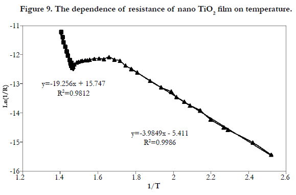
Figure 9. The dependence of resistance of nano TiO2 film on temperature.
– At high temperature range, conductivity of film increased due to only heat excitations to jump electrons from valence band to conduction band – this is a range relating to intrinsic conductivity of semiconductor – has value of~3.32 eV, corresponding with bandgap energy of nano TiO2. This result was relevant to the calculated results Eg from UV–Vis absorption spectrum measurement (~ 3.35 eV).
– At low temperature range, conductivity of film was mainly because carriers were created from dopants ionized – this was a range of conductivity as dopants for extrinsic semiconductor – had value of ~ 0.69 eV, corresponding with dopant level, it may be due to unexpected dopants. This was deep level so it had large carrier catching cross-section. These deep centres relate to luminescent process of TiO2, because deep centres usually act as recombinations or effective traps and control life-time of carriers.
Conclusion
Nanocrytalline TiO2 films were prepared by spraying pyrolysis method. Experimental results show that at substrate temperature ranging from 340°C to 460°C with solution concentration from 0.025 to 0.15M, all of them gave TiO2 films condensed on glass substrate. These were anatase single phase, nanocrytalline TiO2 films with high crystalline quality and cleanliness, equivalent to other expensive prepared methods include comparison with commercial products. The films had mesoporous structure with average sizes of crystalline particles were at range 7–10nm which were lightly dependent on starting-solution concentration and prepared temperature. This method gave nano TiO2 films with small particle size and high stability in comparison with other methods. Characteristic studying results showed that the obtained nano TiO2 films sufficiently exposed typical photoelectric characteristics of TiO2 semiconductor material. Characteristic parameters such as absorption spectrum, luminescent spectrum, bandgap size were suitable and equivalent to data of other authors. Therefore spraying pyrolysis method with simple equipments, used inexpensive and available materials enables to prepare nano TiO2 films with high quality to meet demands of fundamental and applied researches. This method is able to apply in industrial production.
References
- Abou-Helal MO, Seeber WT (2002) “Preparation of TiO2 thin films by spray pyrolysis to be used as a photocatalyst”. App. Surf. Sci 195: 53 – 6.
- Arshak K, Corcoran J, Korostynska O (2005) “Gamma radiation sensing properties of TiO2, ZnO, CuO and CdO thick film pn-junctions”. Sensors and Actuators A 123: 194 – 198.
- Castillo N, Olguin D, Conde-Gallardo A (2004) “Structural and morphological properties of TiO2 thin films prepared by spray pyrolysis”. Rev. Mex. Fis 50(4): 382 – 387.
- Conde-Gallardo A, García-Rocha M, Hernández-Calderón I, Palomino- Merino R (2001) “Photoluminescence properties of the Eu3+ activator ion in the TiO2 host matrix”. Appl. Phys. Lett 78: 3436 – 3438.
- Cristina S. Enache, Joop Schoonman, Roel van de Krol (2006) “Properties of Carbon-doped TiO2 (Anatase) Photo-Electrodes”. Mater. Res. Soc. Symp. Proc 885: 0885-A10.
- Elena Vigil, José A Ayllón, Ana M Peiró, Rafael Rodríguez-Clemente, Xavier Domènech, et al. (2001) “TiO2 Layers Grown from Flowing Precursor Solutions Using Microwave Heating”. Langmuir 17: 891 – 896.
- Garzella C, Comini E, Tempesti E, Frigeri C, Sberveglieri G (2000) “TiO2 thin films by a novel sol-gel processing for gas sensor applications”. Sensors and Actuators B 68: 189 – 196.
- Gümüş C, Ozkendir OM, Kavak, Ufuktepe Y (2006) “Structural and optical properties of zinc oxide thin films prepared by spray pyrolysis method”. J. Optoel. and Adv. Mater. 8(1): 299 – 303.
- Hasan MM, Haseeb ASMA, Saidur R, and Masjuki HH (2008) “Effects of Annealing Treatment on Optical Thin Films Properties of Anatase TiO2”, Proceeding world academy of science, engineering and technology 30: 221 –225.
- http://kuroppe.tagen.tohoku.ac.jp/~ecd/museum-j.htm
- Jae P Lee, Mi H Park, Taek-Mo Chung, Yunsoo Kim, Sung Myung M (2004) “Atomic Layer Deposition of TiO2 Thin Films from Ti(OiPr)2(dmae)2 and H2O”. Bull. Korean Chem. Soc 25(4): 475 – 479.
- Madhusudan Reddy K, Gopal Reddy CV, Manorama SV (2001) “Preparation, characterization, and spectral studies on nanocrystalline anatase TiO2”. Journal of Solid State Chemistry 158: 180 – 186.
- Lee J, Tanaka T, Uchiyama S, Tsuchiya M, Kamiya T (1997) “Broadband double-layer antireflection coatings for semiconductor laser amplifiers”,Japanese Journal of Applied Physics 36(2): L52 – L54.
- Lei Y, Zhang LD (2001) “Fabrication, characterization, and photoluminescence properties of highly ordered TiO2 nanowire arrays”. J. Mater. Res 16(4): 1138 – 1144.
- Masao Katayama, Shinya Ikesaka, Jun Kuwano, Yuichi Yamamoto, Hideomi Koinuma, et al. (2006) “Field-effect transistor based on atomically flat rutile TiO2”. Appl. Phys. Lett 89(24): 242103-242103.
- Mogyorósi K, Dékány I, Fendler JH (2003) “Preparation and Characterization of Clay Mineral Intercalated Titanium Dioxide Nanoparticles”. Langmuir 19(7): 2938 – 2946.
- More AM, Gunjakar JL, Lokhande CD (2008) “Liquefied petroleum gas (LPG) sensor properties of interconnected web-like structured sprayed TiO2 films”, Sensors and Actuators B 129: 671 – 677.
- Nickolay Golego, Studenikin SA, Michael Cocivera (2000) “Sensor Photoresponse of Thin-Film Oxides of Zinc and Titanium to Oxygen Gas”. J. Elec. chem. Soc 147(4): 1592 – 1594.
- Pravin S Shinde, Pramod S Patil, Popat N Bhosale, Chandrakant H Bhosalew (2008) “Structural, Optical, and Photoelectrochemical Properties of Sprayed TiO2 Thin Films: Effect of Precursor Concentration”. J. Am. Ceram. Soc 91(4): 1266 – 1272.
- Rachel Cinnsealach, Gerrit Boschloo, Nagaraja Rao S, Donald Fitzmaurice (1999) “Coloured electrochromic windows based on nanostructured TiO2 films modified by adsorbed redox chromophores”. Solar Energy Materials and Solar Cells 57(2): 107 – 125.
- Sathyamoorthy R, Sudhagar P, Chandramohan S, and Vijayakumar KP (2007) “Photoelectrical properties of crystalline titanium dioxide thin films after thermo-annealing”. Crys. Res. Tech 42(5): 498 – 503.
- The-Vinh Nguyen, Hyun-Cheol Lee, O-Bong Yang (2006) “The effect of pre-thermal treatment of TiO2 nano particles on the performance of dyesensitized solar cells”. Solar Energy Materials & Solar cells 90: 967 – 981.
- Thierry Cassagneau, Janos H Fendler, Thomas E Mallouk (2000) “Optical and Electrical Characterizations of Ultrathin Films Self-Assembled from 11-Aminoundecanoic Acid Capped TiO2 Nanoparticles and Polyallylamine Hydrochloride”. Langmuir 16: 241 – 246.
- Xinming Qian, Dongqi Qin, Qing Song, Yubai Bai, Tiejin Li, et al. (2001) “Surface photovoltage spectra and photo electrochemical properties of semiconductor-sensitized nanostructured TiO2 electrodes”. Thin solid films 385(1-2): 152 – 161.