Fabrication and Magnetoresistance of Single Au-Ni-Au Nanowire
S. Ishrat1*, K. Maaz2, S. Karim2
1 Department of Physics, COMSATS Institute of Information Technology, Lahore 54000, Pakistan.
2 Nanomaterials Research Group, Physics Division, PINSTECH, Nilore, Islamabad, Pakistan.
*Corresponding Author
S. Ishrat
Department of Physics,
COMSATS Institute of Information Technology,
Lahore 54000, Pakistan.
E-mail: isultana@ciitlahore.edu.pk
Article Type: Research Article
Received: April 29, 2014; Accepted: May 27, 2014; Published: May 29, 2014
Citation: S. Ishrat, K. Maaz, S. Karim. (2014). Fabrication and Magnetoresistance of Single Au-Ni-AuNanowire, Int J Nano Stud Technol, 03(02), 45-49. doi: dx.doi.org/10.19070/2167-8685-140009
Copyright: S. Ishrat© 2014 This is an open-access article distributed under the terms of the Creative Commons Attribution License, which permits unrestricted use, distribution and reproduction in any medium, provided the original author and source are credited.
Abstract
Magnetoresistance of Au-Ni-Aunanowire with 300 nm long nickel segment sandwiched between the gold segmentsis studied. Structural analysis of the sample is performed by X-ray diffraction and transmission electron microscopy, which reveals the pure phase, crystalline behavior of the nanowires. Magnetic measurements of the samples confirm ferromagnetic behavior due to the presence of nickel in the wires. Current versus voltage measurement of single nanowire bridged between the two gold electrodes shows ohmic behavior at room temperature with a resistance of 73 Ω. Magnetoresistance as a function of the applied field shows a decreasing trend of resistance below 140 Oe, followed by an increasing trend in resistance in the field range 140 Oe<H<250 Oe, and finally attains a saturation value for the fields ≥250 Oe. The results have been explained with reference to the variation of magneto-resistance upon the alignment of spins, formation of magnetic domains and their propagation along the direction of magnetic field.
2.Introduction
3.Experimental
4. Results and Discussion
6.Conclusion
7.Acknowledgment
8.References
Key Words
Magnetoresistance; Nickel Nanowires; Coercivity; Electrochemical Deposition.
Introduction
One dimensional quasi-nanostructures exhibit unique physical and chemical properties, due tohigh aspect ratio, finite size, and quantum confinement effects. Due to these unique properties metallic and semiconductor nanowires have gained immense interest for their practical applications in recent technologies. Size dependent magnetic properties e.g. magnetization measurement and anisotropy behavior of ferromagnetic (FM) materials have been widely studied in recent years. Nickel (Ni) is ferromagnetic material in its bulk form with randomly oriented moments in the absence of external magnetic field. When the external magnetic field is applied to nickel its spin alignment takes place along the direction of applied field that changes its resistance substantially due to the scattering of charge carries from the grain boundaries depending on the microstructure and magnetic domains [1].
Magneto-transport measurements performed on single nanowire can provide precise information about the spin dependent properties rather than bunch of the nanowires. Due to dipolar interactions between the adjacent nanowires, bunch of nanowires can’t provide the satisfactory information [2]. According to Mott model, electrical conductivity in metals is described in terms of two independent conduction channels formed by the spin up and spin down electrons with different resistance of these channels. In multisegment nanowires of Au/Ni/Au the spins in Ni segment are aligned in such a way that the magnetic moment of Ni layer is pointing along the applied field direction. While in the absence of magnetic field the spins are randomly aligned with respect to one another that can increase the overall resistance of the material. So the conduction channel electrons can experience less resistance in the presence of external magnetic field because of the spins which are aligned, while in the absence of the field these electrons experience enhanced resistance due to the spins, which are randomly, aligned [3].
Among various techniques used for the fabrication of FM nanowires template assisted synthesis is one of most common technique in which the nanowires are grown in polycarbonate or alumina (AAO) templates by using DC electrochemical deposition technique. In this technique the nanowires are fabricated by depositing their ions into the pores of the membranes [4].
In this work, we have studied structural, magnetic, and magnetoresistive properties of single Au/Ni/Au nanowire bridged between the two gold electrodes. Magnetization hysteresis loops of the wires embedded in AAO templates have been recorded using SQUID-VSM at an applied field of 2 kOe. Magnetoresistance (MR)of single nanowire was investigated by using 4K Helium closed cycle system under varying (positive and negative) magnetic fields. Ferromagnetism has been found to arise from Ni, which is sandwiched between the two Au segments while MR in these nanowires has been found to arise as a result of the spin alignment taking place under varying magnetic fields.
Experimental
Segmented nanowires were fabricated by electrochemical deposition in porous anodized aluminum oxide (AAO) templates. AAO served as scaffold template with a pore diameter of 200 nm and thickness of about 13 mm. For the growth of multisegment nanowires backside of AAO template was made conductive by electron beam evaporated (EBM) evaporated silver (Ag). A three electrode DC cell was used for the deposition process, where an Ag/AgCl was used as the reference electrode, platinum as the counter electrode, and AAO template with thermally evaporated conductive Ag layer served as working electrode. A thin sacrificial Ag layer of ~2 µm was electrodeposited for the uniformity of cathode surface; gold plating solution was used for the deposition of Au segments while Ni sulfate solution was used for Ni deposition in the nanowires. In the entire deposition process, a potential of -0.95 V was maintained across the working and reference electrode. The length of each segment was tuned by controlling the deposition time and quantity of exchange charge during the fabrication process. After the deposition of the wires the template was kept in nitric acid for 15 min to remove the silver layer deposited prior to the wire fabrication, and later on the AAO template was dissolved in NaOH solution (3 molar) for 45 min. In order to separate NaOH from the nanowires the samples were rinsed 5 times with deionized water and then centrifuged to get the clear wires. Further details of fabrication are given in our previous work [5]. After cleaning the wires they were dispersed on Si/SiO2 wafer for the fabrication of electrodes. The electrodes were fabricated by using photolithography. Current-voltage (I-V) measurements were performed to study the ohmic contacts of the wires. Structural analyses were performed by TEM and optical microscopy, while the composition of nanowires was analyzed by X-ray diffraction (XRD) and energy dispersive X-ray spectroscopy (EDX).
Results and Discussion
Schematic diagram for the entire fabrication process is shown in Fig. 1(a-f). Fig. 1(a) shows the top view of AAO templates with uniform cylindrical pores across the templates, while Fig.1(b) shows these templates with silver layer deposited by EBM evaporator and a thin sacrificial Ag layer was electrochemically deposited for making the uniformity of working electrodesurface. Fig.1(c) shows the deposition of first gold segment by using chrono-amperometry technique. In the next step, Ni is deposited on the top of Au segment as shown in Fig.1 (d), which is to be sandwiched between the two gold segments as shown in Fig.1 (e). Finally, after the removal of silver layer by using HNO3 and then the host template from the nanowires, the free standing nanowires are obtained as shown in Fig. 1(f). For the fabrication of uniform nanowires throughout the length of the template, the pore size is very important because the diameter of the wires mainly depends on the pore size of the templates, while the uniformity of the wire depends on the pore surface of the templates [4,5].
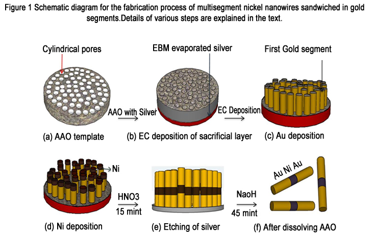
Figure 1. Schematic diagram for the fabrication process of multisegment nickel nanowires sandwiched in gold segments. Details of various steps are explained in the text..
Figure 2(a-c) shows the TEM images of the as-fabricated nanowires after liberating them from their host template. The cylindrical shape and uniform cross-section of the wires with 200 nm diameter is clear in TEM image as shown in Fig. 2(a), while Fig. 2(b) shows a single segment nanowire where a Ni segment of length 300 nm is clearly seen to be sandwiched between the two Au segments with an overall diameter of 200 nm. In Fig. 2(c) interface between Ni and Au segments with bright and dark contrasts are shown, which is quite clear and uniform in this case. The crystalline nature of the as prepared nanowires was investigated by XRD after liberating them from their host templates and then dispersing on Si wafer. XRD pattern of the wiresas shown in Fig 3(a) confirms the pure phase, crystalline nature of the wires. In XRD pattern there is no extra peak, which confirms the purity of the prepared nanowires. Fig. 3(b) shows EDX of nanowires which also confirms that nanowires are composed of purely Ni and Au without any impurities.
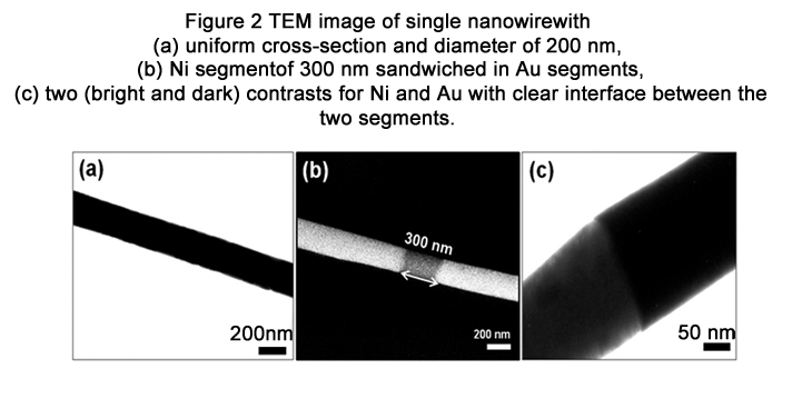
Figure 2. TEM image of single nanowirewith (a) uniform cross-section and diameter of 200 nm, (b) Ni segmentof 300 nm sandwiched in Au segments, (c) two (bright and dark) contrasts for Ni and Au with clear interface between the two segments.
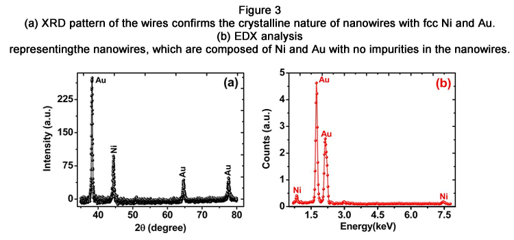
Figure 3 (a) XRD pattern of the wires confirms the crystalline nature of nanowires with fcc Ni and Au. (b) EDX analysis representingthe nanowires, which are composed of Ni and Au with no impurities in the nanowires.
Magnetization hysteresis M(H) loop of the nanowiresis shown in the Fig. 4. The nanowires were left embedded in AAO template for magnetic measurements, while for structural characterization they were liberated from AAO template and dispersed on silicon wafer. Magnetic measurement has been taken at room temperature underan applied field of 2 kOe. The coercivity (Hc) of 300 nm Ni sandwiched in Au segments is 140 Oe. A study of magnetic measurements at room temperature for similar nanowires has been reported in our previous article [5]. The ferromagnetic behavior is expected to arise mainly from the Ni content in the nanowires, which is about 300 nm long sandwiched in Au segments in this case. Crystalline nature of 300 nm long Ni segment in these nanowires is reported to be multicrystalline and multidomain [5]. From Fig. 4 it is seen that the M(H) loop is not saturated at 2 kOe or even at higher fields that can be attributed to the surface effects in these nanowires similar to the case of ferrite nanoparticles where such behavior is observed due to the pronounced surface effects at the nanoscale [6].
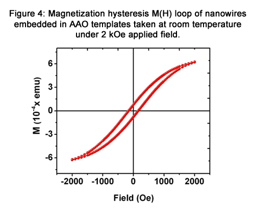
Figure 4 Magnetization hysteresis M(H) loop of nanowires embedded in AAO templates taken at room temperature under 2 kOe applied field.
I-V measurement of single nanowire bridged between two gold electrodes is shown in Fig. 5 with two SEM images of different resolutions in the inset. SEM images show that the single nanowire captured between two gold electrodes with a gap of ~2 μm. In order to make contacts of the wire photolithography technique was used. The metal deposition was employed by using EBM evaporator with chromium and gold of 25nm and 200 nm thicknesses, respectively. The resistance of the wire calculated from I-V curveis 73Ω at room temperature. Fig. 6 shows the magnetoresistance (MR) as a function of the field applied along the length of the wire (longitudinal direction) at room temperature. The arrows in the figure indicate the direction of the applied field. From Fig. 6, it is seen that for the fields >250 Oe the resistance of the wire saturates in both directions. For smaller fields (140 Oe<H<250Oe) the resistance decreases with decreasing field followed by a peak in MR at Hc= ±140 Oe, which is symmetric in both directions. On further decreasing the field below Hc= ±140 Oe the MR value is going to increase symmetrically, and finally attains a value of its room temperature resistance (i.e. 73 Ω). In this case, the nucleation process is mainly responsible for magnetization reversal in the lower field region (i.e. below 140 Oe). Similar behavior of MR at low fields has also been observed for grating of nanowires and single nanowire deposited in polycarbonate membranes that has been attributed to magnetization reversal processes in the nanowires [7,8]. In the low field region, as the field increases it nucleates various magnetic domains, which are stationary and pinned at the interface between the two domains (domain walls). To unpin these spins from the domain walls and move (propagate) them, higher fields (i.e. above 140 Oe) are required, where Hc=±140 Oe are the fields at which the resistance minima are observed in our case. These minima at Hc =±140 Oe correspond well with the coercivity values determined from the M(H) curve of the same nanowires shown in Fig. 4. Thus, below Hc the spins are aligned parallel to the field direction thereby forming the spin-channels for the flow of charges which effectively decrease the MR values as shown in Fig. 6. At higher fields (>±140 Oe) the already developed domains propagate along the field direction.From Fig. 6, it is seen that in the range 140-250 Oe MR symmetrically increases and attains a saturation value of 74Ω. This is attributed to the behavior of the spin dependent scattering and mixing of spin channels as a result of the mistracking of the electrons precession at the domain walls [9-11]. Another possibility of the increasing magnetoresistance at the domain walls may be the opposite magnetization between the adjacent domains which can lead the spin accumulation that relaxes by spin-flip scattering over the spin diffusion length that results in the enhancement of magnetoresistance at the domain walls. In this case, the spin accumulation over a short distance can cause the mistracking effects, which enhances the magnetoresistance in the nanowire. In the high field region >250Oe the magnetoresistance saturates and becomes independent of the applied field as shown in Fig. 6. In this case both processes (nucleation and propagation of domains) are expected to complete and no further chance of scattering and mistracking of electrons are taking place in Ni segment, suggesting a stable magnetoresistance at higher fields.
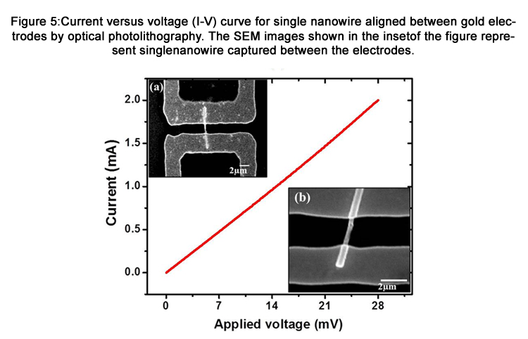
Figure 5 Current versus voltage (I-V) curve for single nanowire aligned between gold electrodes by optical photolithography. The SEM images shown in the insetof the figure represent singlenanowire captured between the electrodes.
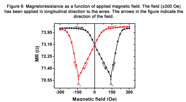
Figure 6 Magnetoresistance as a function of applied magnetic field. The field (±300 Oe) has been applied in longitudinal direction to the wires. The arrows in the figure indicate the direction of the field.
Conclusions
In this work, magnetoresistance of a single Au-Ni-Au nanowire fabricated by electrochemical deposition have been investigated. XRD and TEM confirmed the crystalline nature of the nanowires, while the EDX confirmed the quantitative presence of Ni and Au with no impurities in the wires. M(H) loop of nanowires embedded in the templates confirmed that ferromagnetism arises as a result of Ni content in the wires. I-V characterization showed the ohmic behavior of the nanowire, while magnetoresistance as a function of applied field followed a decreasing trend below 140 Oe. This is attributed to the formation of magnetic domains (spins channels) that allow the charge carriers to flow along the direction of applied field. The increasing trend of resistance in the high field region (140-250 Oe) is ascribed to the spin dependent scattering and mixing of spin channels that increase MR in this field range. Finally, the saturation of scattering and mistrackingeffects results in the constant MR values at higher fields (i.e. above 250 Oe).
Acknowledgment
This research was supported by World Class University program funded by the Ministry of Education, Science and Technology through the National Research Foundation of Korea (R32-10204).
References
- J. Sarkar, G.G. Khan, A. Basumallick, Bull. Mater (2007) Sci. 30(271).
- S. J. Hurst, E.K. Payne, L. Qin, C.A. Mirkin( 2006) Angewandte Chemie International Edition.45 (2672).
- B. Yoo, Y. Rheem, W.P. Beyermann, N.V. Myung(2006) Nanotechnology. 17(2512).
- N.V.Hoang, S.Kumar, Gil-Ho Kim(2009) Nanotechnology, 20(125607).
- S.Ishrat, K.Maaz, C. Rong, S.H. Kim, M.H.Jung , et.al.(2012)Current Applied Physics 12 (65).
- K. Maaz, A. Mumtaz, S.K. Hasanain, M.F. Bertino(2010) Journal of Magnetism and Magnetic Materials, 322(2199).
- C.Shearwood, S.J.Blundell, M.J.Baird, J.A.C.Bland, M.Gester, et.al.( 1994) J.Appl.Phys. 75(10) (5249).
- R. Ferre, K. Ounadjela, J.M. George, L.Pireaux, S.Dubois,(1997) Phys. Rev. B 56(21) ( 14066).
- J.F. Gregg, W.Allen, K. Ounadjela, M. Viret, M. Hehn,et.al(1996) Phys. Rev. Lett., 77 (1580).
- M. Viret, D. Vignoles, D. Cole, J.M.D. Coey(1996) Phys. Rev. B 53(8464–8468).
- P.M. Levy, S.Zhang(1997) Phys. Rev. Lett.79(5110).