ZnO nanowire gas sensor with UV-light for improved sensitivity
T.S.van den Heever1*,G.L.Hardie1,W.J.Perold1
1 Department of Electrical and Electronic Engineering, Stellenbosch University, Stellenbosch,Western Cape, 7601,South Africa
*Corresponding Author
T.S.van den Heever
Department of Electrical and Electronic Engineering,
Stellenbosch University, Stellenbosch,Western Cape,
7601, South Africa.
E-mail: tsvdh@sun.ac.za
Article Type: Research Article
Received: February 25,2013; Accepted: March 29, 2013; Published: April 22, 2013
Citation: van den Heever TS, G. L. Hardie, W. J. Perold. (2013). ZnO nanowire gas sensor with UV-light for improved sensitivity, Int J Nano Stud Technol, 2(1), 12-16. doi: dx.doi.org/10.19070/2167-8685-130003
Copyright: van den Heever TS© 2013 This is an open-access article distributed under the terms of the Creative Commons Attribution License, which permits unrestricted use, distribution and reproduction in any medium, provided the original author and source are credited.
Abstract
ZnO nanowires are synthesised on a patterned substrate in order to see the response to different gases. Under
ambient conditions the sensor shows very little response to any gas. A UV-light source is used to increase the sensitivity of the sensor by increasing the conductivity of the ZnO nanowires. The UV-light decreases the number of oxygen ions present on the surface of the ZnO nanowires which leads to better sensitivity. The sensor, with the aid of the laser, can distinguish between the different gases that were used, argon, oxygen, carbon dioxide and nitrogen. When a mixture of two gases was used the response fell in between the response of the individual gases. The obtained results are repeatable and consistent over different sensors.
2.Introduction
3.Experimental Section
4. Results and Discussion
5.Conclusion
6.References
Key Words
ZnO; Nanowires; Gas Sensor; UV-light.
Introduction
One dimensional nanostructures, like nanowires or nanotubes, are increasingly being used for different sensing applications. This is due to the high surface to volume ratio which aims to increase the sensitivity of these devices [14]. The main problem is that most of these sensors are used at temperatures above 100C to increase sensitivity, which limits its application [5].
Recente advances has been made in the use of UVlight at room temperature to increase the sensitivity of metal-oxide sensors [6]. Different materials are used, with ZnO one of the most studied materials. ZnO is widely used due to its wide band gap of 3.4 eV and ZnO nanowires can be grown at low temperatures, making it suitable for growth on various substrates [5]. ZnO also has high conduction electron mobility and good chemical and thermal stability [7].
In this work a gas sensor is manufactured by growingZnO nanowires on a patterned substrate. The sensor is placed inside a testing chamber to inverstigate the response when different gases are introduced to the chamber. A commercial laser pointer is used to increasethe sensitivity of the sensor to better differentiate between different gasses.
Experimental Section
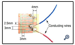
The ZnO nanowires are grown on a substrate - with copper tracks - as illustrated in Figure 1. The substrate is cleaned and RF-sputtering is then used to deposit a 40 nm to 50 nm layer of ZnO onto the entire substrate. An aqueous solution of 30 mM zinc nitrate hexahydrate (Zn(NO3)2 6H2O) and 30 mM hexamethylenetetramine (HMTA) is prepared. The substrate is placed, coated side downward, on top of the solution.The solution is then placed in an oven at 85C for ZnO nanowire growth [8,9]. After 8 hours the substrate is removed, rinsed with DI-water and dried with nitrogen gas. Nanowire growth is removed in two areas to solder conducting wires to the substrate. The nanowire growth is characterised by a Phenom Fei Desktop SEM [10].
Figure1: Graphical representation of the patterned substrate used for nanowire growth with copper used for the pattern.
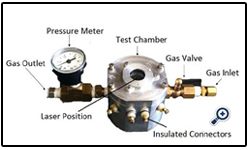
The substrate is placed inside a small testing chamber to see the effect different gasses have on the resistance of the nanowires. Figure 2 shows the setup: a solid aluminium chamber, single gas inlet and outlet and a laser-pointer attached at the top. The substrate is connected to a LabJack U6 [11] analog to digital converter to display the data on a computer screen. The laser is driven by connecting it to a Protek DDS function
Figure2: Chamber used for testing the sensor. Gas inlet and outlet pipes are on the side with the laser fixed on the top.
Results and Discussion
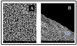
Figure 3 shows the typical nanowire growth. Figure 3(a) is a top view of the nanowires showing the growing direction, density and the average diameter, measured to be 80 nm to 100 nm. Figure 3(b) is a cross-sectional view of the nanowires, also showing the growth is perpendicular to the substrate with an average length 1μm to1.5μm.
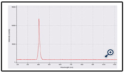
The sensor has minimal to no response when gas is introduced to the system. This is because the resistance is already so large that a small change is not noticeable. It is thus necessary to reduce the resistance in order to see when a small change occurs. The resistance is reduced when the sensor is exposed to light. The resistance of ZnO nanowires decrease by four to six orders of magnitude when exposed to UV-light in the 380 nm wavelength range [13]. The ZnO nanowires have a strong UV emission peak - attributed to nearbandedge emission - at 385 nm [14-16]. Therefore, a commercial available laser pointer, at a wavelength of 400 nm, was chosen as UV-source. Figure 4 shows a measurement of the wavelength of the laser pointer.
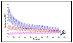
The photons of the laser have energy at 3.1 eV, just belowthe band gap of ZnO (3.37 eV), causing exciton transition which leads to an increase in conductivity because electronhole pairs are created inside the nanowire, decreasing the depletion layer [14,17,18]. The depletion layer mostly consists of oxygen ions (O-, O2-, O-2 ) on the surface of the nanowire that captures the photo-excited holes and leads to an increase in carrier density and a decrease in resistance [19]. At higher resistance more oxygen ions are present and thus a bigger decrease in the resistance under UV-light will be measured. This is shown in Figure 5: the laser is connected to the function generator with the settings as follow: a square wave with amplitude 9.8 V, frequency of 100 mHz, duty cycle of 50% and an offset of 100%.
Figure 3: SEM pictures of (a) a top view and (b) a side view of the ZnOnanowires grown on the substrate.
The response of the nanowires is measured when the laser is turned on at different resistance values. At the higher resistance value a bigger drop is observed because there are more oxygen ions to interact with the photons, compared to the lower levels. At these lower levels most of the oxygen ions are already combined with holes and hence equilibrium is reached, or close to it. There is a clear linear relationship between the starting resistance and the response to the UVlight: at higher resistance the response is quick and gradually reduces as the resistance reduces.
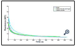
Different gasses are added to the system, while still pulsing the laser, and the data is plotted. Figure 6 shows the resulting plot for five cases: no gas, argon, oxygen, nitrogen and carbon dioxide. From Figure 6 it is clear that all four gasses have different responses and it differs from the no-gas case.
Each gas has a different rate of decrease in resistance over the first 200 seconds before flattening out and reaching a stable resistance. It is thus possible to differentiate between different gasses by looking at the reduction of the resistance during the first stage or looking at the resistance value once steady state has been reached.
The difference in response is attributed to surface reactions. When then laser is turned on, the depletion layer is reduced as described above. The passing gas interacts with the oxygen ions on the nanowire surface which decreases the oxygen species on the surface of the nanowire and increases the electron concentration [20]. Each gas has a different effect on the concentration of oxygen ions on the surface of the nanowire which leads to a difference in the conductivity. Oxidizing gases decreases conductance of n-type semiconductors and can be seen as oxygen and carbon dioxide has the highest steady state resistance apart from the no-gas case. The behaviour is ambient conditions are still higher due to the high level of intrinsic oxygen ions present on the nanowire plus the added ions due to the oxygen in air. The gases inject electrons into the conduction band of the nanowire which further increases the conductivity [21]. Hence, the resistance is lower for all the cases where gas is introduced into the chamber, compared to the no-gas case.
Oxidizing gases leads to an increase in the resistance because it adds more oxygen ions to the nanowires. The response to argon and nitrogen is believed to be due to the lack of oxygen in the chamber which leads to a decrease in the number of oxygen ions due to the laser and no reaction with the gas takes place. This means more electrons are injected into the nanowire and the conductivity increases. The observed difference between argon and nitrogen is unknown. Argon is a noble gas and no interaction between argon and the nanowires is present. As mentioned, the response is due to the lack of oxygen in the chamber rather than interaction with the argon. Nitrogen forms a very weak bond with the ZnO nanowires, compared to oxygen which forms a more stable bond, which leads to a slight increase in resistance compared to the argon case by a far lower resistance compared to the oxygen case [22]. Next the sensor was tested for repeatability. The same tests were performed a couple of days from each other. The obtained results were within the error margin (less than 5%), showing good, repeatable data from the sensor. Figure 7 shows the response of a second sensor that was manufactured using the same method. The response is again very similar to the first sensor meaning the measurements are repeatable and similar over different senors.
FIgure 5: Measured response of ZnO nanowire sensor when the UV-light is pulsed starting at different resistance values. It is clear that the biggest response is at the higher resistance and the response decreases as the resistance decreases.
FIgure 6: Measured response of the ZnO nanowire sensor when different gasses are added to the chamber while pulsing laser. It is clear that all the gases result in different response of the sensor.
FIgure 7: Measured response of another sensor when different gasses are added to the chamber while pulsing laser. The results are very similar to the ones obtained with the first sensor.
The last test was to see the effect when a mixture of the gases was introduced to the system. Figure 8 shows the response when a 1 : 1 mixture of carbon dioxide and argon is introduced to the system. During the first 100 seconds the response is the same as the response to argon, due to the lack of oxygen in the chamber. After the 100 seconds the response falls in the middle of argon and carbon dioxide as the nanowires react the the oxygen, before the response starts to follow the carbon dioxide line. During the first part the argon dominates and there are little interactions between the carbon dioxide and the nanowire. As the time progresses the carbon dioxide starts to react with the nanowireswhich leads to an increase in the resistance. This test was also repeated days apart as well as with different sensors and the response remained the same. The test was also performed with a mixture of argon and oxygen and again the resulting graph fell between the two separate cases. This means the sensor can be used for gas sensing where more than one gas is being used.
Figure 8: Measured response of the gas sensor when a mixture of carbon dioxide and argon is introduced to the system. The response of the mixed gas falls in the middle of the two seperate gases.
Figure 9: Measured recovery of the sensor to the maximum resistance value in ambient conditions. The recovery time is much larger than the reponse time to the different gases.
The sensor has two big draw bakcs. The fisrt problem with the sensor is the recovery time. Figure 9 shows the recovery of one sensor. The resistance of the sensor was reduced by the laser and then left in ambient conditions to recover back to its maximum value. The recovery time is more than 4000 seconds, which is much longer than the sensing time for the different gases (in the order of 200 seconds). In order to use the sensor for gas sensing the recovery time has to be decreased drastically. The second problem is the area where the laser is shined. If the laser is moved to a new position, the response is very different. It is thus necessary to keep the laser and sensor aligned at all times to ensure the response will be the same.
Conclusion
ZnO nanowires were grown on a patterned substrate to use as a gas sensor. A UV-light source, at 400 nm, was used to enhance the sensitivity of the sensor. The UV-light decreases the amount of oxygen ions on the surface of the nanowire which in turn increases the conductivity. Different gases were introduced to the system and the response was measured. The sensor showed different responses to the different gases. Each gas has a different response due to a difference in the interaction with the ZnO nanowires. Oxidising gases has the highest resistance over time and a oxygen deprived state has the lowest resistance. The results are also repeatable and only small differences exist between different sensors. Lastly the sensor was used to detect a mixture of gases and the response was a combination of the separate gases. ZnO nanowires can be used in gas sensing application but the recovery time has to be reduced in order to make it a viable sensor.
References
- R. J. Chen, R. Franklin, N., J. Kong, J. Cao, W. Wombler, T., Y. Zhang,and H. Dai, “Molecular photodesorption from single-walled carbon nanotubes,” Applied Physics Letters, vol. 79, p. 2258, 2001.
- G. Collins, P., K. Bradley, M. Ishigami, and A. Zettl, “Extreme oxygen sensitivity of electronic properties of carbon nanotubes,” Science, vol. 287, p. 1801, 2000.
- Y. Cui, Q. Wei, H. Park, and M. Lieber, C., “Nanowire nanosensors for highly sensitive and selective detection of biological and chemical species,” Science, vol. 293, p. 1289, 2001.
- F. Favier, C. Walter, E., P. Zach, M., T. Benter, and M. Penner, R., “Hydrogen sensors and switches from electrodeposited palladium mesowire arrays,” Science, vol. 293, p. 2227, 2001.
- S. Fan, K. Srivastava, A., and P. Dravid, V., “Uv-activated room temperature gas sensing mechanism of polycrystalline zno,” Applied Physics Letters, vol. 95, p. 142106, 2009.
- E. Comini, A. Cristalli, G. Faglia, and G. Sberveglieri, “Light enhanced gas sensing properties of indium oxide and tin dioxide sensors,” Sensors and Actuators B, vol. 65, p. 260, 2000.
- A. Nekoubin and A. Nekoubin, “Design an electrical nose with zno nanowire arrays:,” World Academey of Science, Engineering and Technology, vol. 58, p. 1007, 2011.
- L. Vayssieres, “Growth of arrayed nanorods and nanowires of zno from aqueous solutions,” Advanced Materials, vol. 15, p. 464, 2003.
- M. Willander, L. L. Yang, A. Wadeasa, S. U. Ali, M. H. Asif, Q. X.Zhao, and O. Nur, “Zinc oxide nanowires controlled low temperature growth and some electrochemical and optical nanodevices,” Journal of Materials Chemistry, vol. 19, p. 1006, 2009.
- PhenomWorld. [Online]. Available: http://www.phenom-world. com/
- LabJack. [Online]. Available: http://labjack.com/u6
- Protek. [Online]. Available: http://www.protektest.com/main.asp
- H. Kind, H. Yan, B. Messer, M. Law, and P. Yang, “Nanowire ultraviolet photodetectors and optical switches,” Advanced Materials, vol. 14, p.158, 2002.
- L. Luo, Y. Zhang, S. S. Mao, and L. Lin, “Fabrication and characterization of zno nanowire based uv photodiodes,” Sensors and ActuatorsA, vol. 127, p. 201, 2006.
- J. Liu, N. Motta, and S. Lee, “Ultraviolet photodetection of flexible zno nanowire sheets in polydimethylsiloxane polymer,” Beilstein Journal of Nanotechnology, vol. 3, p. 353, 2012.
- A. Umar, B. Kim, J. Kim, and Y. B. Hahn, “Optical and electrical properties of zno nanowires grown on aluminium foil by non-catalytic thermal evaporation,” Nanotechnology, vol. 18, p. 175606, 2007.
- W. I. Park, Y. H. Jun, S. W. Jung, and G. C. Yi, “Excitonic emissions observed in zno single cyrstal nanorods,” Applied Physics Letters, vol. 82, p. 964, 2003.
- Y. C. Kong, D. P. Yu, B. Zhang, W. Fang, and S. Q. Feng, “Ultraviolet- emitting zno nanowires synthesised by a physical vapor deposition approach,” Applied Physics Letters, vol. 78, p. 407, 2001.
- Q. H. Li, Q. Wan, Y. X. Liang, and T. H. Wang, “Electronic transport through individual zno nanowires,” Applied Physics Letters, vol. 84, p. 4556, 2004.
- Q. Wan, H. Li, Q., J. Chen, Y., H. Wang, T., L. He, X., P. Li, J., and L. Lin, C., “Fabrication and ethanol sensing characteristics of zno nanowire gas sensors,” Applied Physics Letters, vol. 84, p. 3654, 2004.
- S. Kar, N. Pal, B., S. Chuadhuri, and D. Chakravorty, “One-dimensional zno nanostructures arrays: sythesis and characterization,” Journal of Physical Chemistry B, vol. 110, p. 4605, 2006.
- M. Breedon, J. S. Spencer, M., and I. Yarovsky, “Adsorption of atomic nitrogen and oxygen on zno(2110) surface: a density function theory sudy,” Journal of Physics: Condensed Matter, vol. 21, p. 144208,2009.

