Investigation of Structural, Morphological, Electronic and Optical Propertiesof Au Irradiated Ni Doped ZnO Thin Films prepared by Pulsed Laser Deposition
Hanif H, Murtaza G*, Arif HS
Centre for Advanced Studies in Physics, GC University, Lahore, Pakistan.
*Corresponding Author
Ghulam Murtaza,
Centre for Advanced Studies in Physics,
GC University, Lahore-54000, Pakistan.
Tel: +92-3214263536
E-mail: gmrai@gcu.edu.pk
Received: August 07, 2016; Accepted: October 15, 2016; Published: October 20, 2016
Citation: Hanif H, Murtaza G, Arif HS (2016) Investigation of Structural, Morphological, Electronic and Optical Propertiesof Au Irradiated Ni Doped ZnO Thin Films prepared by Pulsed Laser Deposition. Int J Magn Nucl Sci. 2(4), 24-33.
Copyright: Murtaza G© 2016. This is an open-access article distributed under the terms of the Creative Commons Attribution License, which permits unrestricted use, distribution and reproduction in any medium, provided the original author and source are credited.
Abstract
In this research work, effect of Au ions irradiated Zn1-xNixO (with x = 0.0, 0.02, 0.04 and 0.06) thin films grown by pulsed laser deposition on Si substrate has been investigated. The influence of ions implantation on structural, optical, electronic and morphological properties of the thin films have been examined by X-ray diffraction (XRD), X-ray absorption near edge spectroscopy (XANES),Field emission scanning electron microscopy (FESEM) and ultraviolet-visible (UV-Vis) spectroscopy. XRD results confirm the existence of single phase hexagonal wurtzite structure of ZnOin all the thin films. The preferred orientation were observed along (002) plane. It has also been analyzed that due to co-doping of Au ions and Ni ions, the peaks shifts towards the shorter angle, as a result,lattice expansion has been identified. UV-Vis measurements reveal that the band gap decreases up to x = 0.02 and 0.04 Ni concentration, after that it starts increasing at x= 0.06. XANES analysis reveals the presence of Zn, Ni and O at different edges, K and L edges.FESEM results reveal that the surface morphologies are scarcely changed.
2.Introduction
3.Experimental Detail
4.Results and Discussion
4.1.XRD Analysis
4.2.Optical Analysis
4.3.Morphology
4.4.Electronic Properties
5.Conclusion
6.References
Keywords
Pelletron Accelerator; Au-Ni co doping; XANES; UV-Vis Spectroscopy.
Introduction
II-IV metal oxide i.e.,Zinc Oxide (ZnO)intrinsically n-type semiconductor whichis the most pioneer, topical, everlasting and extensively utilized academic and industrially researchedmaterial. It has unique, inherent and versatile properties such as direct wide band gap up to 3.4eV, binding energy of 60 meV, low price, environment friendly nature, natural abundance, chemical as well as thermal stability andnon-toxic nature [1]. It possesses experimentally a stable hexagonal wurtzite crystal structure. Such properties make ZnO a promising material for diverse device applications such as optoelectronic,blue and ultraviolet optical devices [2, 3], varistors, solar cell [2, 4], gas sensor,surface acoustic wave devices, photodetectors [5], heat mirror for energy saving [6], nanolasers, transparent conducting films [7], laser diodes [8], biomaterials, window material for display, cosmetics, light emitting diodes [10], biomedical application [10], sunscreens [11] and spintronics [12].
In order to establish more versatility in one of the application spintronics, II-IV alloys can be doped by a minute amount of transition metal (Ni, Mn, Co, Cu, Ti, Sc, V, Cr and Fe etc) and rare earth (Eu, Gd, Sm, La, Ce and Eretc) metals. The non-magnetic semiconductor such as ZnO result into a new material called diluted magnetic semiconductors (DMS). Among oxide based DMS, ZnO is vastly utilized material because its intrinsic room temperature ferromagnetism is attained by doing process [13]. Magnetic property is attributed to the d electron interaction with the s or p electron of the host material. In the latest investigation on DMS still p-type conduction is under discussion and n-type conduction has been explored vastly. Ferromagnetism at and above room temperature has been studied in diverse materials. Although, it is a great achievement in the field of semiconductor technology, still lot of work is required to synthesis and confirm the basic phenomenon for the magnetism in ZnO wide band gap semiconductors.
Several techniques have been employed to fabricate ZnO thin films that including pulsed laser deposition (PLD) [14], sol-gel [15], RF magnetron sputtering [16], chemical vapor deposition (CVD) [17, 18], spray pyrolysis [19], chemical bath deposition [20], molecular beam epitaxy (MBE) [21], organic chemical vapor deposition (MOCVD) [22] and DC magnetron sputtering [23]. Among these entire thin film fabrication techniquesPLD is most versatile physical vapor deposition technique that is utilized for achieving high quality and featured thin films with low deposition temperature. Recently, Mn, Sb, Ni, Cd, Co, Er and Mg doped ZnO thin films have been investigated successfully [14, 15, 20, 24-28]. However, Ni doped ZnO is more promising candidate for its attaining room temperature ferromagnetism.
Similarly, doping Cu, Ag and Au into the ZnO has been of great interest [29-31]. It has been observed that doping of different elements into the ZnO thin film is an effective approach to improve diverse properties. Introducing Au into ZnO is a typical way used to enhance gas sensing properties. However, by Au ion implantation, conductivity of the thin films can be enhanced. It is given that by Au doping p-type conductivity of ZnO can be achieved [32-35]. Ion implantation is a well-known material engineering technique, in which implanted dopants are introduced into the thin film by the bombardment with ions,in order to modify the surface properties of material in a controlled way. One of the merits of the ion implantation is that every material can be used as a dopant for ion implantation. In the present study, Au ion irradiated Ni doped ZnO thin films have been successfully prepared by the PLDon Si(100) substrate and its structural, morphological, electronic and optical properties are investigated by diverse characterization techniques.
Experimental Detail
The precursors used were ZnO and NiOpowder (99.9 % purity, Sigma Aldrich) and Au ions source.A series of thin films have been fabricated by three steps. Initially, solid state reaction method was performed for Zn1-xNixO (with x= 0.0, 0.02, 0.04, 0.06) pellet formation.Appropriate stoichiometric ratios of ZnO and NiO powders were weighed, mixed, grinded, and calcined in air at 500°C for 3 h in furnace (Nabertherm Model). The calcined powders were again ground by adding a small amount of poly vinyl alcohol (PVA). The ground powders were then used for the formation of pellets having 5mm thickness and 1.6 cm diameter using hydraulic press at 6 ton. The prepared pellets werefinally sintered at 1100° C in furnace for 6 h. In second step, thin films were deposited onultrasonically cleaned Si (100) substrate by using pulse laser deposition (PLD). To ablate the ZnNiO target Nd: YAG laser (YG981C-10, Quantel France)of 2nd harmonics (λ=532 nm) was used. The ambient gas was O2 and the working pressure of the chamber was 15 m torr(7.5×10⁻² torr). The parameters chosen for deposition of thin films were as, pulse duration of 6ns, repetition rate of 10 Hz, number of shots 6000, power of 200 mJ and target to substrate distance of 3cm. The substrate temperature and thin film deposition time employed was 300°C and 10 minrespectively. The incident angle for the laser beam was 45˚ with respect to the target. Before depositing the thin films, substrate was first cleaned ultrasonically in distilled water and acetone. Finally, thin films were deposited on silicon substrate Si (100) in high vacuum.
In the third step, Au ions of 500 KeVenergy with fluence 2×10¹⁴ ions/cm2 were irradiated by using Pelletron accelerator (6SDH-2, NEC). The beam size for irradiating Au singly charged ions was 2×2 cm2. All the samples were irradiated at room temperature under high vacuum condition. The prepared thin films were characterized by different techniques, such as, XRD (2D Phaser bruker model) for structural analysis, UV-Vis spectroscopy (Perkin Elmer’s UV/VIS/NIR lambda 950 spectrophotometer) for determining the band gap of thin films. XANES (1D beam line in Pohang source) was performed for scrutinizing the electronic structure. FESEM (Nova Nano SEM) was utilized for investigating film surface morphology.
Results and Discussion
Figure 1 displays X-ray diffraction pattern of Au+ ion irradiated Zn1-xNixO (x= 0.0, 0.02, 0.04, 0.06) n-type Si (100) substrate. It is evident that preferred orientation of the dominant intensity peak in all ion irradiated thin films either doped or codoped is along (002) at angle 34.6630. It is observed that all diffracted peaks match with JCPDS data card number 01-089-1397 having hexagonal wurtzite ZnO structure. It is also revealed from the spectra that secondary phase of Au2O3 (with the JCPDS data card number 00-043-1039) having orthorhombic structure were observed at angle 25˚in Au+ ion irradiated Zn1-xNixO (x = 0.0, 0.02, 0.04, 0.06) thin films. This exhibits the fact that Au+ ions are partially incorporated into the ZnO crystal lattice and are partially reside on the film surface which created defects in the crystal structure, this is due to the fact that ionic radius of Au3+ (0.84 Å) is greater than theZn (0.74 Å). Peaks of the Au+ ion irradiated Zn1-xNixO (with x= 0.0, 0.02, 0.04, 0.06) thin films are shifted towards lower angle as compared to pristine ZnO as shown in Figure 1. The reason for the shifting of peak towards lower angle is the ionic radius of the Zn (0.74 Å) that is smaller than the Au3+ (0.84 Å). Irradiating Au+ ions in Zn1-xNixO causes the lower angle shifting of (002) peak, this is unusual, usually peaks shifted towards larger angle which is due to codoping effects and creates the expansion in the ZnO matrix as well [36]. In various studies it has been reported that as contrast to pure ZnO, (002) ZnNiO peak has been shift towards larger angle [37-39] and Ni ions has been incorporated into the ZnO matrix attributed by the fact that Ni ionic radius (0.69Å) is smaller than the ZnO (0.74Å). By using XRD data lattice constants of the Pure ZnO, Au+ ion irradiated ZnO and Zn1-xNixO were calculated by using cell software and presented in Table 1. Results show that lattice parameter ‘a’ and ‘c’ increases gradually with Ni doping. It is noted that the lattice parameters depend upon diverse factors; quantity of disparate impurity atoms, defects, distinction between ionic radii of doped ions (Ni, Au) and host material, such as, ZnO etc., [40, 41]. An increase in lattice parameters of Au+ ion irradiation Zn1-xNixO thin film with diverse Ni contents is depicted in Figure 2. Figure reveals that lattice parameters ‘a’ and ‘c’ increases with increasing Ni contents. Because ionic radius of Ni (0.69 Å) is smaller than the Zn2+ ( 0.74 Å)[42], so an increase in the lattice parameters confirm the incorporation of the Ni2+ ions at the interstitial places in the crystal lattice [43]. Crystallite size (D) of all the samples has been calculated using the Scherrer’sequation as given below [44] and summarized in Table 1.
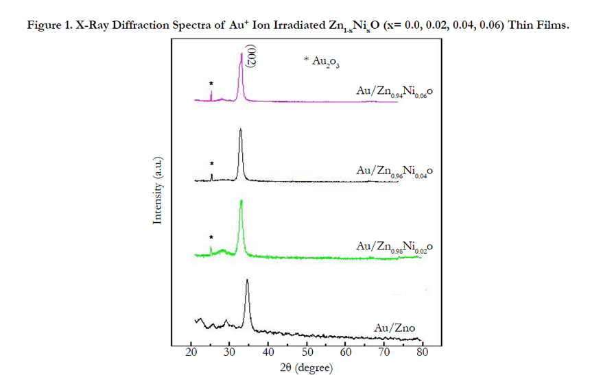
Figure 1. X-Ray Diffraction Spectra of Au+ Ion Irradiated Zn1-xNixO (x= 0.0, 0.02, 0.04, 0.06) Thin Films.
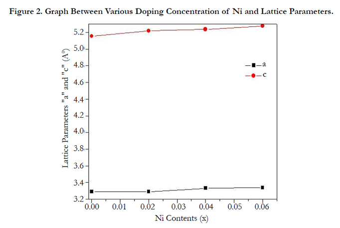
Figure 2. Graph Between Various Doping Concentration of Ni and Lattice Parameters.
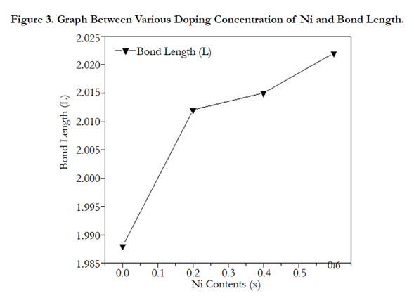
Figure 3. Graph Between Various Doping Concentration of Ni and Bond Length.
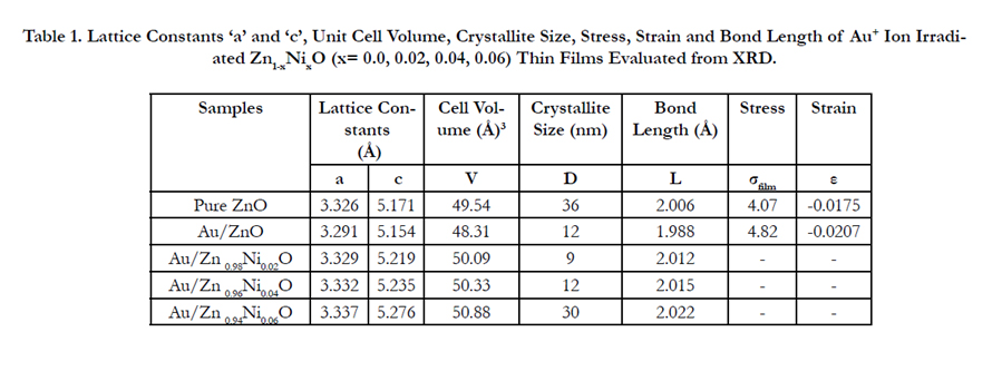

Table 1. Lattice Constants ‘a’ and ‘c’, Unit Cell Volume, Crystallite Size, Stress, Strain and Bond Length of Au+ Ion Irradiated Zn1-xNixO (x= 0.0, 0.02, 0.04, 0.06) Thin Films Evaluated from XRD.
Here D is the crystallite size in nanometer, k is the Scherrer’s constant equal to 0.89, λ is the wavelength of the X-ray, β is the FWHM (full width half maximum) in radians and θ is the half diffracted angle. It has been found that crystallite sizeof the Au+ ion irradiated Zn1-xNixO thin film increases by increasing Ni contents. An increase in the crystallite size reveals the fact that crystallinity of the thin film has been enhanced. It also shows the fact that Ni atoms are being incorporated in the interstitial sites and there is a difference in the ionic radius of the Zn2+ (0.74 Å) and Ni (0.69 Å). A decrease in the crystallite size of the ZnAuO thin film is due to ion irradiation.
The bond length (L)[43] of Zn-O for Au+ ion irradiated Zn1-xNixO (with x= 0.0, 0.02, 0.04, 0.06) respectively, has been calculated using equation 2 and given in Table 1.
Where u is the positional parameter and the value of u for wurtzite structure is given below
The calculated data has been used to plot the graph for bond length verses doping concentration of Ni shown in Figure 3. It has been observed that with the increase in Ni contents bond length increases as presented in Table 1. From XRD data lattice parameters has been calculated, then by using lattice parameters volume of the unit cell has also been calculated by using following formula.
Figure 4 is a graph between doping concentration and volume of the unit cell. It has been noticed that with the increase in doping contents of Ni volume increases gradually. This increase in volume is attributed to the fact that when peaks shifted towards lower angle lattice expansion occurs and volume increases. Similarly, strain in the c-axis was computed by using XRD data by using formula shown in equation 5 [43].
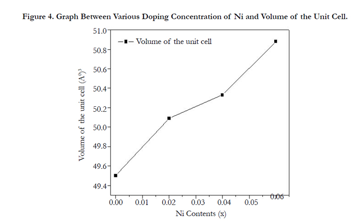
Figure 4. Graph Between Various Doping Concentration of Ni and Volume of the Unit Cell.
Where cfilm the lattice parameter (c) of ZnO thin film and cbulk is the lattice parameter (c) of ZnO Pellet (bulk). Calculated strain value is ε=-0.0175. Strain produced is negative so strain is compressive hence lattice expands. Also this value of strain reveals the fact that as we move from bulk to thin film there is some strain due to defects. Also from the above results stress in the thin films has been computed by using the biaxial formula.
Stress in the films is presented in the Table 1. Stress that has been observed is tensile because it is positive stress. Stress is due to the reason that by ion irradiation additional stress is generated because energy has been transferred from ion irradiation into the ZnO lattice. So the stress is intrinsic which has been observed due to the defects and impurities in the thin film. Stress in all other samples has not calculated because their pellet XRD has not done.
Ultraviolet Visible spectroscopy (UV-Vis) is one of the characterization technique used to approximate the band gap of the Au+ ion irradiated Zn1-xNixO (x= 0.0, 0.02, 0.04, 0.06). In the UV-V is spectroscopy at reflection mode, on room temperature measurements was executed on all the samples in the UV-V is spectral region. The reflectance spectra of ZnO pellet, ZnO and Au ion irradiated Zn1-xNixO (with x= 0.0, 0.02, 0.04, 0.06) Si(100) substrate thin films was obtained by using UV-V is spectroscopy. The Figure 6 depicts the UV-Vis reflection spectra of ZnO pellet and Au ion irradiated Zn1-xNixO (x= 0.0, 0.02, 0.04, 0.06) thin films. Band gap of the ZnO pellet and Au ion irradiated Zn1-xNixO (x= 0.0, 0.02, 0.04, 0.06) thin films was calculated by using KubelkaMunk function F(R) [41, 45, 46] given in the following equation.
Here F(R) is the KubelkaMunk function and R is the reflectance. Energy (hv) is calculated by using the formula given below.
Here λ is the wavelength. By using data obtained from the UVVis spectroscopy graphs has been plotted energy (hv) in eV verses [F(R)hv]2. In order to evaluate the direct band gap of all the samples the spectra curve is extrapolated to [F(R)hv]2=0 [47, 48]. The extrapolated band gap energies Egof ZnO pellet, ZnO and Au ion irradiated Zn1-xNixO (x= 0.0, 0.02, 0.04, 0.06) thin films are exhibited in the Figure 5. The determined values of the bandgap energy of ZnO pellet and Au ion irradiated Zn1-xNixO (x= 0.0, 0.02, 0.04, 0.06)thin films are presented in Table 2.
The band gap of ZnO pellet and Au ion irradiated Zn1-xNixO (x= 0.0, 0.02, 0.04, 0.06) thin films exhibit varying trend. The bandgap of the ZnO pellet obtained by extrapolating the UV-V is spectra is 3.06 eV. While the band gap of the Zn1-xNixO (x= 0.0, 0.02, 0.04, 0.06) thin films first decreases by increasing doping concentration up to x= 0.04 and then band gap increases by increasing up to x= 0.06. This decrease in the band gap is attributed to the red shifting and increase to the blue shifting. The red shift in the Au ion irradiated Zn1-xNixO thin films with Ni doping concentrations (x= 0.0, 0.02, 0.04, 0.06) is associated with the sp-d exchange interaction. The variation in the band gap has also been elucidated by the alteration of the lattice parameter because of the doping effect. It has been found that as lattice parameters increases the band gap decreases. This band gap decreasing effect closely relate to our experimental results of XRD, as lattice parameters are increasing [47-49]. As well as by increasing Ni concentration further up to x= 0.06 a blue shift has been observed.
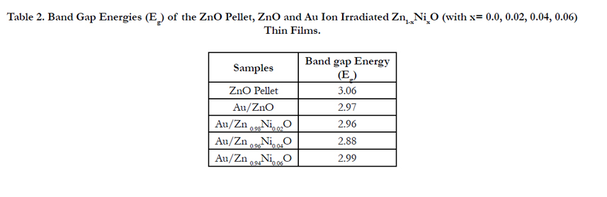
Table 2. Band Gap Energies (Eg) of the ZnO Pellet, ZnO and Au Ion Irradiated Zn1-xNixO (with x= 0.0, 0.02, 0.04, 0.06)
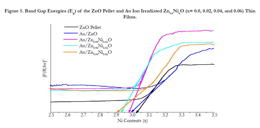
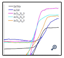
Figure 5. Band Gap Energies (Eg) of the ZnO Pellet and Au Ion Irradiated Zn1-xNixO (x= 0.0, 0.02, 0.04, and 0.06) Thin Films.
FESEM is utilized for the analysis of the morphology of the thin film and it gives the resolution upto 1 nm. The representative images of the ZnO, Au/ZnO and Au/Zn 0.96Ni0.04O thin films shown in the Figure 6(a) along with Au/Zn 0.96Ni0.04O EDX spectrum (Figure 6(b)) have been given. Figure 7 represents the ellipsometric data, which have been used to obtain the thickness of the ZnO thin films. The data clearly depicts that the thickness of the thin film is ~ 180nm. SEM results reveal that the flakes formation with Au irradiation have been observed in these representative images. Study shows that flakes are formed due to the Exfoliational sputtering phenomena. After irradiating the Au ions on the Zn1-xNixO thin films, the morphology of the thin film is changed throughout and channeling or interconnected microstructures are observed in the thin films. Channeling is due to ion induced heating, melting, bond breakage and resolidification. This channeling clearly shows that re-solidification has occurred and channels have formed in the representative graphs as shown in the Figure 6(a). It has been also predicted that in Au/ZnO image only channel or interconnected microstructures are observed and in Au/Zn1-xNixO image channels as well as resolidification occurs [50]. Qualitative and quantitative analysis of EDX spectra clearly reveals the presence of Zn, O, Ni and Au in the Au/Zn 0.94Ni0.06O thin film.
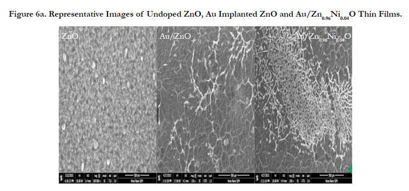
Figure 6a. Representative Images of Undoped ZnO, Au Implanted ZnO and Au/Zn0.96Ni0.04O Thin Films.
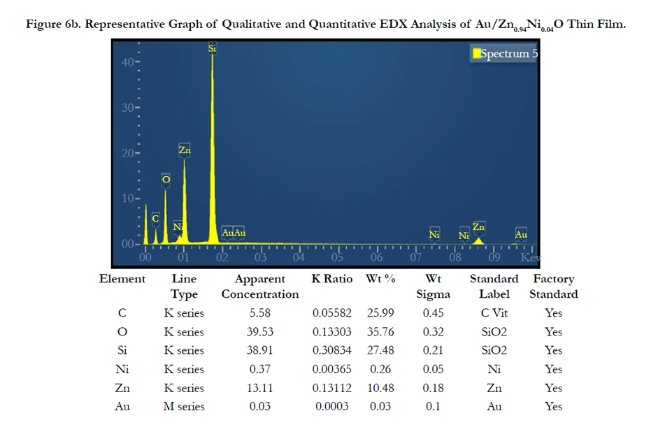
Figure 6b. Representative Graph of Qualitative and Quantitative EDX Analysis of Au/Zn0.96Ni0.04O Thin Films.
For the investigation of the electronic structure such as oxidation state and coordination environment etc. of the material XANES [51] is utilized. K-edge spectra is obtained by transition from 1s level to p level and L2,3 edge spectra by 2p to s or d level. When electron is absorbed from the 2p1/2 and 2p3/2 level L2 and L3 edge are formed. XANES has been performed on Au ion irradiated Zn1-xNixO thin films as shown in the Figure 8 – 10.
From the normalized O k-edge spectra of XANES as shown in the Figure 8, it is revealed that the pre-edge is from 530-533 eV. Pre-edge energy peak for (with x = 0.0, 0.02) is at 531eV and at (x= 0.4) pre-edge is at 535 eV. For (x= 0.6) the pre-edge peak is at 531 eV. Pre-edge elucidates the hybridization of oxygen 2p state with transition metal (Ni2+) 3d. White line region ranges from 535-540 eV. The intensity of the white line peak is high for the bulk sample ZnO and intensity of white line at (x= 0.0, 0.02, 0.04, 0.06) is 538 eV as well as at x=0.04 is 539 eV. An increase in the intensity of the white line has been scrutinized in the Au ion irradiated Zn1-xNixO thin films as compare to the bulk ZnO thin film.
Normalized Ni L2, 3 edges XANES spectra is shown in Figure 9. The electronic configuration of Ni2+ is [Ar] 3d84s2. The 3d shell in Ni is not completely filled but 4s is completely filled. Ni give rise to L2, 3 because transition takes place from 2P1/2 and 2P3/2 to unoccupied 3d level giving rise to L2 and L3 edge respectively. These transitions are the source of white line spectra in XANES. Spectra have three regions in Ni L2, 3 edges no change has been observed in region A in all films. Region B and C is at 856 eV and 874 eV respectively, no change has been observed in this also. This spectrum confirms the presence of the Ni in all the samples. A normalized XANES spectrum of hexagonal Zn has been depicted in Figure 10. Zn has electronic configuration [Ar] 3d104s2. It has 3d shell completely filled. Transition in Zn2+ have been take place from 2p core level (spin-orbit split into 2p1/2 and 2p3/2 levels, giving rise to L2 and L3 edges, respectively) to empty electronic state above the Fermi level cause the white lines. Region A is at 1030 eV, region B is in the range 1039-1055 eV and region C is in the range 1059-1064 eV respectively. Region B corresponds to L3 edge and C to L2 respectively.
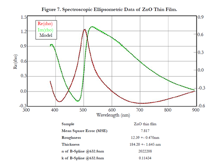
Figure 7. Spectroscopic Ellipsometric Data of ZnO Thin Film.
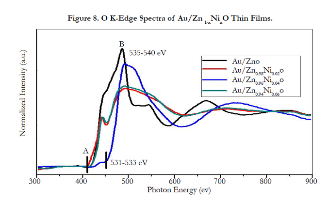
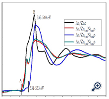
Figure 8. O K-Edge Spectra of Au/Zn1-xNixO Thin Films.
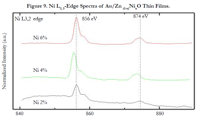
Figure 9. Ni L2, 3-Edge Spectra of Au/Zn (1-x)NixO Thin Films.
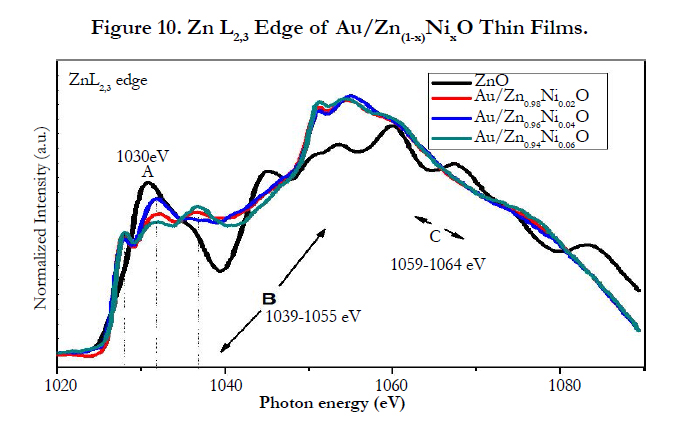
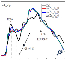
Figure 10. Zn L2,3 Edge of Au/Zn (1-x)NixO Thin Films.
Conclusion
Successfully Au ion irradiated Zn1-xNixO (x= 0.0, 0.02, 0.04, 0.06) thin films have been grown on Si (100) substrate by PLD. Au/ Ni doping effect on the structural, optical, morphological and electronic structure properties have been examined. For the structural analysis XRD is performed which reveals the preferred orientation of the as deposited thin films along (002) plane. A secondary phase of Au2O3 has been found in the thin films which disclose that ions are not completely incorporated into the thin films but are residue on the thin films and hence produce defects in the thin films. An increase in the crystallite size has been found in the thin films, this increase is due to the difference in the ionic radius of the Zn2+ (0.74 Å) and Ni (0.69 Å) and also reveals that crystallinity has enhanced. Peaks are shifted towards the smaller angle as a result the lattice expansion occurs. Volume of the films has been calculated which increases by increasing Ni contents. Bond length has been observed to be increase by increasing Ni contents. Strain and stress has also been found in the thin films due to the shifting from bulk to the thin film.
A UV-Vis analysis result in the reduction in the bandgap of the thin films has been found. The band gap of the thin films first decreases, when the content of the Ni are low and then it increases by increasing Ni contents. The morphology of the thin films has been investigated by FESEM which reveals that the defects are produced on the surface of the thin film due to ion irradiation. XANES confirms the presence of the Ni, Zn, O in the ion implanted thin films.The successful incorporation of Ni and Au into ZnO lattice will definitely enhance the magnetic properties of ZnO and hopefully this will be the best material for spintronics application.
References
- G Kaur, A Mitra , K Yadav (2015) Growth And Properties Of Pulsed Laser Deposited Al-doped ZnO Thin Film. Adv mater lett. 6(1): 73-79.
- D Hernández-Socorro, Z Montiel-González, S Rodil-Posada, L Flores-Morales, H Cruz-Manjarrez, et al., (2012) Effect of 8MeV Si ions irradiation and thermal annealing in ZnO thin films. J Crys Grow. 354 :169-173.
- S Kurtaran, S Aldag, G Ofofoglu, I Akyuz, F Atay, Transparent conductive ZnO thin films grown by chemical spray pyrolysis: the effect of Mg. J Mater Sci: Materials in Electronics. 1-8.
- M Chaari, A Matoussi, Z Fakhfakh (2011) Structural and dielectric properties of sintering zinc oxide bulk ceramic. MSA. 2(7): 764.
- X Yan, D Hu, H Li, L Li, X Chong (2011) Nanostructure and optical properties of M doped ZnO (M= Ni, Mn) thin films prepared by sol–gel process. Physica B: Condensed Matter. 406 (20): 3956-3962.
- E Dumont, B Dugnoille, S Bienfait (1999) Simultaneous determination of the optical properties and of the structure of rf-sputtered ZnO thin films. Thin Solid Films. 353 (1): 93-99.
- H Kim, F Lugo, S Pearton, D Norton, YL Wang n (2008) Phosphorus doped ZnO light emitting diodes fabricated via pulsed laser deposition. Appl Phys Lett. 92 (11): 112108.
- T Meron, G Markovich (2005) Ferromagnetism in colloidal Mn2+-doped ZnO nanocrystals. J Phys Chem B. 109(43): 20232-20236.
- N Doğan, A Bingölbali, L Arda (2015) Preparation, structure and magnetic characterization of Ni doped ZnO nano-particles. J Magn Magn Mater. 373: 226-230.
- V Kumar, V Kumar, S Som, L Purohit, O Ntwaeaborwa (2014) Role of swift heavy ions irradiation on the emission of boron doped ZnO thin films for near white light application. J Alloys and Comp. 594 : 32-38.
- T A Dar, A Agrawal, R Choudhary, P Sen (2015) Electrical and magnetic transport properties of undoped and Ni doped ZnO thin films. Thin Solid Films. 589: 817-821.
- S Major, K Chopra, (1988) Indium-doped zinc oxide films as transparent electrodes for solar cells Solar energy materials. 17 (5): 319-327.
- U Wahl, E Rita, J Araújo, E Alves, J Correia (2003) Implantation site of rare earths in single-crystalline ZnO . Appl Phys Lett. 8: 1173-1175.
- YF Hsiou, WK Hung, CW Wang (2015) Fabrication of Sb-doped p-type ZnO Thin Films by Pulsed Laser Deposition. Atlas J Materl sci. 2(1): 60-64.
- R Govindaraj, R Govindan, M Geetha, P Anbarasan (2015) Structural, morphological and luminescence studies on pristine and La doped zinc oxide (ZnO) nanoparticles. Optik-Int J Light Electr Opti. 126(17): 1555-1558.
- V Şenay, S Pat, Ş Korkmaz, T Aydoğmuş, S Elmas (2014) ZnO thin film synthesis by reactive radio frequency magnetron sputtering. Appl Surf Sci. 318: 2-5.
- JC Hsiao, CH Chen, HJ Yang, CL Wu, CM Fan (2013) Highly textured nO:B films grown by low pressure chemical vapour deposition for efficiency enhancement of hetrojunction silicon based solar cells. J Taiwan Inst Chemi Eng. 44 (2013): 758-761.
- M Islam, M Hossain, S Razzak, M Haque, D Saha (2016) Effect of Deposition Time on Nanostructure ZnO Thin Films Synthesized by Modified Thermal Evaporation Technique. J Nanosci Nanotechnol. 16 (9): 9190-9194.
- CC Yu, WH Lan, KF Huang (2014) Indium-Nitrogen Codoped Zinc Oxide Thin Film Deposited by Ultrasonic Spray Pyrolysis on n-(111) Si Substrate: The Effect of Film Thickness. J Nanomater. 1-4.
- T Morita, S Ueno, T Tokunaga, E Hosono, Y Oaki, et al., (2015) Fabrication of Transparent ZnO Thick Film with Unusual Orientation by the Chemical Bath Deposition. Cryst Growth Des. 15 (2015) 3150-3156.
- M Suja, SB Bashar, MM Morshed, J Liu (2015) Realization of Cu-Doped p-Type ZnO Thin Films by Molecular Beam Epitaxy. ACS Appl Mater Interfaces. 7 (16): 8894-8899.
- X Cai, H Liang, X Xia, R Shen, Y Liu, et al., (2015) Influence of Cu dopant on the structure and optical properties of ZnO thin films prepared by MOCVD. J Mater Sci Mater Electron. 26 (3): 1591-1596.
- B Wen, C Liu, N Wang, H Wang, S Liu, et al., (2015) Properties of borondoped ZnO thin films deposited by pulsed DC magnetron sputtering at different substrate temperatures Applied Physics A. 121(3): 1147-1153.
- SF Shayesteh, R Nosrati (2015) The Structural and Magnetic Properties of Diluted Magnetic Semiconductor Zn1− xNixO Nanoparticles. J Supercond Nov Magn. 28 (16): 1821-1826.
- G Vijayaprasath, R Murugan, G Ravi, T Mahalingam, Y Hayakawa (2014) Characterization of dilute magnetic semiconducting transition metal doped ZnO thin films by sol–gel spin coating method. Appl Surf Sci. 313: 870-876.
- J El Ghoul, N Bouguila, S Gómez-Lopera, L El Mir (2013) Structural and optical properties of nanoparticles (V, Al) co-doped ZnO synthesized by sol– gel processes. Superlattices Microstruct. 64: 451-459.
- P Murmu, J Kennedy, B Ruck, J Leveneur (2015) Structural, electronic and magnetic properties of Er implanted ZnO thin films. Nucl Instrum Methods Phys Res B. 359(2015): 1-4.
- V Devi, M Kumar, D Shukla, R Choudhary, D Phase, et al.,(2015) Structural, optical and electronic structure studies of Al doped ZnO thin films. Superlattices Microstruct. 83: 431-438.
- N Hongsith, C Viriyaworasakul, P Mangkorntong, N Mangkorntong, S Choopun (2008) Ethanol sensor based on ZnO and Au-doped ZnO nanowires. Ceram Int. 34 (2008): 823-826.
- S Hosseini, IA Sarsari, P Kameli, H Salamati (2015) Effect of Ag doping on structural, optical, and photocatalytic properties of ZnO nanoparticles. J Alloys Compd. 640: 408-415.
- WY Li, LX Jiang, GL Yin, YY Wang, ZY u, et al., (2013) Preparation and characterization of ZnO/Cu/ZnO transparent conductive films. Rare Met. 32 (2013): 273-277.
- E Della Gaspera, M Guglielmi, G Perotto, S Agnoli, G Granozzi, et al., (2012) CO optical sensing properties of nanocrystalline ZnO–Au films: Effect of doping with transition metal ions. Sensors and Actuators B: Chemical. 161(1): 675-683.
- CH Chu, HW Wu , JL Huang (2015) Thin Solid Films. (2015).
- N Tarwal, R Devan, Y Ma, R Patil, M Karanjkar, et al., (20012) Spray deposited localized surface plasmonic Au–ZnO nanocomposites for solar cell application. Electrochimica Acta. 72: 32-39.
- Y Xu, B Yao, Y Li, Z Ding, J Li (2014) Chemical states of gold doped in ZnO films and its effect on electrical and optical properties. J Alloys Compd. 585 (4): 479-484.
- S Lin, Z Ye, J Lu, H He, L Chen (2008) Na doping concentration tuned conductivity of ZnO films via pulsed laser deposition and electroluminescence from ZnO homojunction on silicon substrate. Journal of Physics D: Applied Physics. 41 (15): 155114.
- X Wang, L Zhu, L Zhang, J Jiang, Z Yang, et al., (2011) Properties of Ni doped and Ni–Ga co-doped ZnO thin films prepared by pulsed laser deposition.J Alloys Compd. 509 (7): 3282-3285.
- J Jiang, X Wang, L Zhu, Y Zhang, Z Ye, et al., (2012) The effects of of Ni-Na codoping on structure and properties of ZnO films pulsed laser deposition. J Alloys Compd. 513 (2012) 445-448.
- J Jiang, Xt Wang, Lp Zhu, Lq Zhang, Zg Yang (2011) Electrical and magnetic properties of ZnNiO thin films deposited by pulse laser deposition . J Zhejiang Univ Sci B. 12 (7): 561-566.
- G Murtaza, R Ahmad, M Rashid, M Hassan, A Hussnain, et al., (2014) Structural and magnetic studies on Zr doped ZnO diluted magnetic semiconductor. Curr Appl Phys. 14 (2): 176-181.
- T Ivetić, M Dimitrievska, I Gúth, LR Đačanin, S Lukić-Petrović (2012) Structural and optical properties of europium-doped zinc oxide nanopowders prepared by mechanochemical and combustion reaction methods J Res Phys. 36 (2012) 43-51.
- DL Hou, RB Zhao, YY Wei, CM Zhen, CF Pan et al., (2010) Room temperature ferromagnetism in Ni-doped ZnO films. Curr Appl Phys. 10 (1): 124-128.
- G Srinivasan, RR Kumar, J Kumar (2007) Li doped and undoped ZnO nanocrystalline thin films: a comparative study of structural and optical properties. J sol-gel sci technol. 43 (2): 171-177.
- B Cullity (1978) Elements of X- Ray diffraction. (Edn 2), Adisson-Wesley Publishing. USA.
- R Bylsma, W Becker, J Kossut, U Debska, D Yoder-Short (1986) Dependence of energy gap on x and T in Zn1−xMnxSe: The role of exchange interaction. Phys Rev B. 33 (12): 8207.
- AE Morales, ES Mora, U Pal (2007) Use of diffuse reflectance spectroscopy for optical characterization of un-supported nanostructures. Rev Mex Fisica S. 53 (5): 18.
- J Hays, K Reddy, N Graces, MH Engelhard, V Shutthanandan, et al., (2007) Effect of Co doping on the structural, optical and magnetic properties of ZnO nanoparticles. J Phy Condens Matter. 19 (26): 266203.
- JA Mary, JJ Vijaya, M Bououdina, LJ Kennedy, J Daie et al., (2015) Investigation of structural, surface morphological, optical properties and firstprinciples study on electronic and magnetic properties of (Ce, Fe)-co doped ZnO. Phys B Condens Matter. 456: 344-354.
- NF Djaja, DA Montja, R Saleh (2013) The effect of Co incorporation into ZnO nanoparticles. AMPC. 3: 33.
- C Zegadi, K Abdelkebir, D Chaumont, M Adnane, S Hamzaoui (2014) Influence of Sn Low Doping on the Morphological, Structural and Optical Properties of ZnO Films Deposited by Sol Gel Dip-Coating AMPC. 4(5): 93-104.
- C Schnohr, M Ridgway (2015) X-Ray Absorption Spectroscopy of Semiconductors. Springer in Optical Sciences. Springer, Berlin Heidelberg.